Our Products & Services
TeraProbes Inc. provides world’s first non-contact metrology solution for high frequency electronic device and IC and material testing/characterization. Our proprietary test-beds consists of automated probe stations and virtual, contact-less probe tips, enabling -for the first time- automated S-parameter characterization of electronic devices and ICs for the entire mmW and THz bands. TeraProbes probing test-bed is fully-automated, enabling unattended inspection of every single chip on a wafer at the fraction of the current cost. Our disruptive approach embodies the following functionality at the fraction of current cost:
- On-wafer S-parameter measurements in the mmW and THz bands
- No wear-and-tear, eliminating key shortcomings of contact-based microprobes
- Sub-micron alignment repeatability for reliable and repeatable measurements
- Multi-port device and IC characterization enabled by accurate on-wafer calibration
- Universal, cost-effective test-bed for the entire mmW-THz band
Our support services include custom designs of the non-contact probes for your particular application needs.
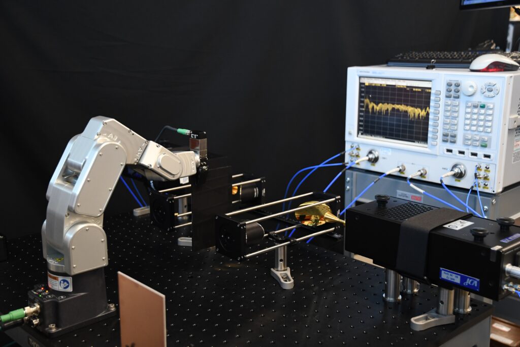
Our material characterization systems use a high-precision robotic arm and a novel calibration to accurately measured the dielectric permittivity and loss tangent of material panels and thin films with 1-in-1000 precision.
We also provide material characterization services using our precision systems.
Please contact us for more information.

TeraProbes Non-contact Probe Station

TeraProbes RoboMat Material Characterization System
Product Line: Non-contact Probing Systems
Our manually-operated non-contact testbed offers reliable, repeatable on-wafer measurements. The wafer under test is aligned manually with precision micromanipulators.
Contactless measurements can also be applied automatically! TP-100-A8025’s imaging processing software and computer controlled manipulators, offer uninterrupted measurements with unprecedented repeatability.
Product Line: Non-contact Robotic Material Characterization Systems
Our quasi-optical material characterization system uses an precision robotic arm to accurately characterize material panels and thin sheets, even painted panels over the entire E-band (60-90GHz).
Our dual-band material characterization system uses a single precision robotic arm and two quasi-optical paths to accurately characterize material panels and thin sheets, even painted panels over the entire E- and F-band (60-140GHz).
